BH1750: a light sensor
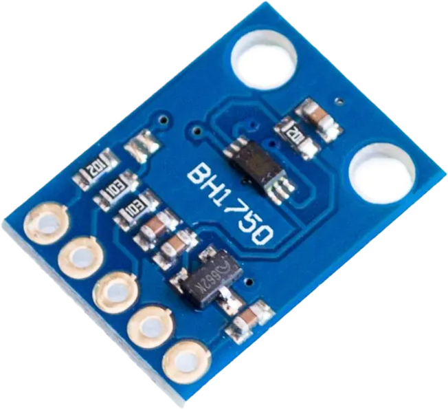
The BH1750 is a digital ambient light sensor that measures light intensity in lux units, providing crucial data for adjusting screen brightness and other device settings according to ambient lighting conditions. Very often this component is put on a breakout board for easy experimentation and usage.
What is Lux?
Lux is a unit of illumination that measures how much light falls on a surface. It is equal to one lumen per square meter.
Some examples of different illuminance levels in lux are:
- 0.0001 lux: Moonless, overcast night sky (starlight)
- 50 lux: Family living room lights
- 1000 lux: Overcast day
- 10,000-25,000 lux: Full daylight (not direct sun)
The human eye can adapt to a wide range of brightness levels, but generally prefers moderate to high illuminance for comfortable vision.
Its wide detection range, from 0 to 65535 lux, mirrors the sensitivity of the human eye to light, making it a versatile tool for various applications.
The breakout board has the BH1750 on it at the center. All information about the BH1750 can be found in the official datasheet. It is always recommended to look this up and check this before working with a new component.
The block diagram
One of the things that's on the datasheet is the block diagram of the BH1750 sensor. This explains what's contained in the integrated-circuit (IC) that makes up the sensor. The list below explains these parts in basic terms.
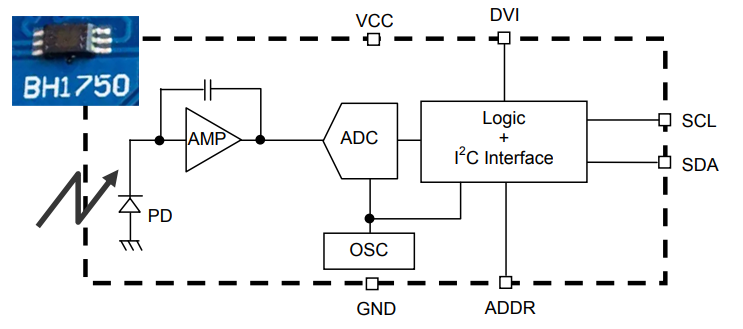
- (PD) Photodiode: The sensor's primary component responsible for converting incident light into electrical current.
- (AMP) Amplifier: Boosts the weak signal from the photodiode to a level suitable for further processing.
- (OSC) Oscillator: Generates the clock signal necessary for the ADC and other internal operations.
- (ADC) 16-bit ADC (Analog-to-Digital Converter): An ADC is a device that takes an electric signal, here from the amplifier, and changes it into a series of numbers that a computer can understand, such as 0's and 1's. The input signal is usually continuous, meaning it can have any value, while the output numbers are discrete, meaning they can only have certain values like 0 or 1 and nothing else. Here the ADC takes the photodiode reading and turn it into a sequence of 0s and 1s.
- Power Down Circuit: Controls the sensor's power state, allowing it to enter low-power modes when not in use.
- Control Logic: Manages the sensor's overall operation, including configuration settings and data transmission.
- I²C Interface Circuit: Facilitates communication between the sensor and external devices via the I²C protocol, enabling seamless integration into various systems.
The pinout of the breakout board
The pinout shows you which parts of the BH1750 in the middle of the board are eventually made available for you to use and connect.
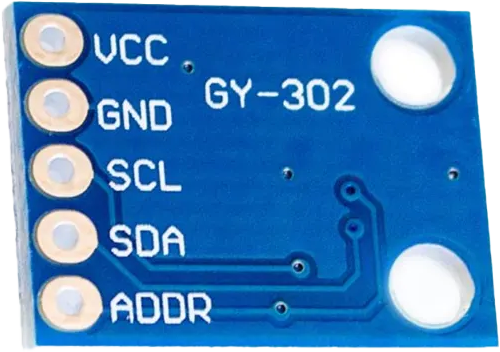
- VCC: This pin is the power supply input, providing the necessary voltage for the sensor to operate.
- GND: Ground pin, which completes the circuit and provides a reference voltage for the sensor, usually 0V.
- SDA: Serial Data pin, used for bi-directional data transfer in the I²C communication protocol.
- SCL: Serial Clock pin, synchronizing data transfer between the sensor and the embedded device in the I²C protocol.
- ADDR: Address pin, allowing selection between two possible I2C peripheral addresses, enabling multiple sensors to coexist on the same bus. On page 10 of the datasheet you can see this functionality. If you apply 0.7 Volts or more to the ADDR pin you need to use the 1011100 I²C address, which is 0x5C in hexadecimal value. if you apply 0.3 Volts or less to the ADDR pin you will need to use 0100011 as the I²C address, which is 0x23 in hexadecimal value.
As you can derive from the lists above, this sensor accurately captures light levels and communicates that data with embedded devices through the embedded communication protocol I²C. We will now look into that.
I²C: embedded communication protocol
I²C, short for Inter-Integrated Circuit, is an embedded communication protocol designed to facilitate data exchange between integrated circuits, such as sensors, displays, and embedded platforms.
While it might seem redundant when considering simple GPIO pins or other protocols, I²C offers distinct advantages, particularly in scenarios where multiple devices need to communicate simultaneously or where a more organized data exchange is necessary. It allows multiple devices to talk to each other using only two wires: one for data and one for clock. It was invented by Philips in 1982 to reduce the number of wires needed to connect different chips on a circuit board.
I²C is useful because it can save space, power, and cost by using fewer wires and pins than other protocols like GPIO or SPI. It also allows devices to have different speeds and voltages, as long as they share a common ground. I²C is widely used in embedded systems.
Imagine I²C as a digital highway connecting various electronic components on a circuit board, like your Orange Pi 3. This highway consists of two lines:
- SDA (Serial Data Line), the SDA line carries the actual data being transmitted.
- SCL (Serial Clock Line),the SCL line provides timing information, like the ticks of a clock, to synchronize the data transfer between devices.
How does I²C work with lines and an Orange Pi 3?
Both SDA (Serial Data) and SCL (Serial Clock) lines are bidirectional, meaning they can be used for both sending and receiving data. Both lines are also open-drain, meaning they are pulled low by the devices and pulled high by external resistors.
To connect an I²C device to an Orange Pi 3, you need to connect the SDA and SCL pins of the device to the corresponding pins on the Orange Pi 3. You also need to connect the ground pins of both devices.
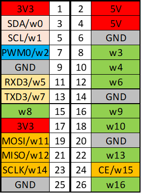
In the context of computer hardware, a "bus" refers to a communication pathway or interface that allows multiple devices to transfer data between each other. The Orange Pi 3 LTS has an I²C bus named I²C0, represented by the pin 3 (SDA) and pin 5 (SCL). The SDA and SCL then need to be connected to the corresponding SDA and SCL of the peripheral.
Serial Data Line (SCL): What is a clock signal and why is it important?
As an analogy, the clock signal is like a conductor orchestrating the flow of traffic on the digital highway. It ensures that data is transmitted and received at the right time, preventing collisions and ensuring orderly communication between devices. Even though you might not be familiar with the concept of a clock in electronics, think of it as a guiding pulse that regulates when information can be sent and received.
Physically a clock signal is a periodic signal that alternates between high and low voltage levels. It is used to synchronize the data transfer between the devices on the I²C bus. The clock signal is generated by the controller device, which initiates and controls the communication. The peripheral devices, which respond to the controller, follow the clock signal and adjust their data bits accordingly.
Language and terms
In older terminology, you will still very often find the controller being called master and the peripheral being called slave.
The clock signal is important for I²C because it ensures that the data bits are correctly aligned and interpreted by the devices. Without a clock signal, the devices would not know when to start or stop sending or receiving data, or how fast to do so. The clock signal also allows the controller to vary the speed of the communication, depending on the capabilities of the peripheral devices. The typical speed of I²C is 100 kHz (standard mode), but it can go up to 400 kHz (fast mode) or even 3.4 MHz (high speed mode).
SDA (Serial Data Line): Transferring packets of Bits and Bytes
Now, let's delve into the data line, where the actual information is transmitted. Data in I²C is organized into packets, which consist of individual bits. A bit is the smallest unit of data and can represent either a 0 or a 1. These bits are grouped together to form bytes, which are collections of 8 bits. Each byte represents a piece of information, such as a sensor reading or a command to control a device.
Bits & Bytes
A bit is a binary digit, which means it can only have two possible values: 0 or 1. These values can be used to represent different things, such as on or off, true or false, yes or no, etc. For example, a light switch can be either on or off, so it can be represented by a single bit: 0 for off and 1 for on.
A byte is a group of 8 bits, which can represent 256 different values. This is because there are 2^8 possible combinations of 0s and 1s in 8 bits. For example, 00000000 is one possible byte, and it represents the value 0. 00000001 is another possible byte, and it represents the value 1. 11111111 is another possible byte, and it represents the value 255. Each byte can be used to store a piece of information, such as a letter, a number, a color, etc. For example, the letter A can be represented by the byte 01000001, and the number 42 can be represented by the byte 00101010.
What is the data line and how does a data packet look like for I²C?
The data line is the line that carries the actual information between the devices on the I²C bus. The data line is connected to the SDA pin of each device. The data line is used to send and receive data bits, which are the smallest units of information. A data bit can be either 0 (low voltage) or 1 (high voltage).
A data packet is a sequence of data bits that forms a meaningful message for the devices. A data packet for I²C consists of several parts:
- Start condition: This is a special signal that indicates the beginning of a data packet. It is generated by the controller by pulling the SDA line low while the SCL line is high.
- Device address: This is a 7-bit or 10-bit code that identifies the peripheral device that the controller wants to communicate with. The controller sends this code on the SDA line, followed by a read/write bit that specifies whether the controller wants to read from or write to the peripheral.
- ACK/NACK: This is a 1-bit signal that indicates the acknowledgement or rejection of the previous data bit. It is generated by the receiver (either the controller or the peripheral) by pulling the SDA line low (ACK) or high (NACK) while the SCL line is high.
- Data byte: This is an 8-bit code that represents the actual data that the controller or the peripheral wants to send or receive. The sender sends this code on the SDA line, followed by an ACK/NACK signal from the receiver.
- Stop condition: This is a special signal that indicates the end of a data packet. It is generated by the controller by pulling the SDA line high while the SCL line is high.
Anatomy of an I²C Data Packet in detail
When devices communicate using I²C, they follow a structured protocol involving several components to ensure reliable data exchange. A typical data packet consists of the following elements:
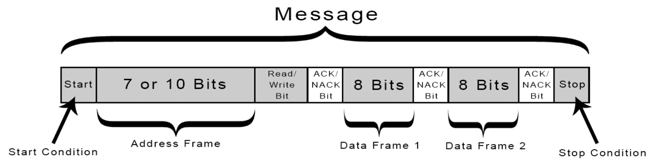
Start condition: The communication begins with a start condition, which is a special signal indicating the initiation of data transfer. For example, the controller device generates a start condition by pulling the SDA line low (moving the voltage from high to low) while the SCL line remains high. So, a start condition might look like this: SDA transitions from high to low while SCL remains high.
Device address: Following the start condition, the controller device transmits the address of the intended recipient device on the SDA line. Let's say the controller wants to communicate with a device with the address
1010 000. Along with the address, the controller also sends a read/write bit indicating whether the subsequent operation is a read or write operation. If it's a write operation, the read/write bit will be0. So, the transmission might look like this:1010 0000(address + write bit).ACK/NACK: After receiving the device address, the recipient device evaluates the address to determine if it matches its own address. If the address matches, the recipient sends an acknowledgment (ACK) signal back to the sender by pulling the SDA line low during the clock pulse following the transmission of the address. So, if the device acknowledges, the SDA line might transition from high to low during the ACK clock pulse.
First Data byte transmission: Following the ACK/NACK phase, the controller device transmits the first data byte (
0100 1101) on the SDA line. Each bit is transmitted sequentially on the SDA line, starting with the most significant bit (MSB) and ending with the least significant bit (LSB). So, the transmission might look like this:0(MSB) ->1->0->0->1->1->0->1(LSB).ACK/NACK for the first Data byte: Upon receiving the first byte of data, the recipient device acknowledges its successful reception by sending an ACK signal or indicates a transmission error by sending a NACK signal. So, if the device acknowledges the first byte of data, the SDA line might transition from high to low during the ACK clock pulse.
Second Data byte transmission: Following the ACK/NACK for the first data byte, the controller device transmits the second data byte (
1110 0011) on the SDA line. So, the transmission might look like this:1(MSB) ->1->1->0->0->0->1->1(LSB).ACK/NACK for the second Data byte: Upon receiving the second byte of data, the recipient device acknowledges its successful reception by sending an ACK signal or indicates a transmission error by sending a NACK signal. So, if the device acknowledges the second byte of data, the SDA line might transition from high to low during the ACK clock pulse.
Stop condition: Once all data bytes have been transmitted and acknowledged, the communication cycle concludes with a stop condition. The controller device generates a stop condition by releasing the SDA line, allowing it to be pulled high (moving the voltage from low to high) by the external pull-up resistor, while the SCL line remains high. So, a stop condition might look like this: SDA transitions from low to high while SCL remains high.
🛠 Connecting and reading out the BH1750 with Orange Pi 3 LTS using I²C
There are a number of steps to get readings from the BH1750 to display on the Orange Pi 3's console:
Enable the I²C interface on the Orange Pi 3 LTS by following section "3.19.3 26pin I2C test" on page 139 of the OrangePi_3_LTS_H6_User Manul_v2.1.pdf listed on Canvas.
Install the
smbusandadafruit-circuitpython-bh1750Python packages usingpip.Write a Python script that imports the
smbusandadafruit_bh1750modules the creates aBH1750object with the I²C address of the sensor.This address is listed on page 10 of the datasheet. We have not applied a voltage to the ADDR pin of the sensor so we will need
0100011(ADDR ≦ 0.3VCC) as the address, which is0x23in hexadecimal value. Note that the possibility to select two addresses allows the user to connect up to two BH1750 sensors on the same I²C bus by using different peripheral addresses.The the code needs to read the light level using the
readLightLevelmethod:
import smbus
import adafruit_bh1750

# Create an I2C bus object
bus = smbus.SMBus(0)

# Create a BH1750 object with the I2C address 0x23
sensor = adafruit_bh1750.BH1750(bus, 0x23)

# Read the light level in lux
light = sensor.readLightLevel()

# Print the result
print("Light: {:.2f} lx".format(light))- Run the code on the Orange Pi 3 LTS with the
pythoncommand. This code will only display values once and then stop. You can edit it yourself with thetiminglibrary to make it publish multiple times.